6 Steps for Optimizing Imaging Systems for Semiconductor Inspection
Semiconductor inspection is both an imaging challenge and a systems-engineering challenge. Whether inspecting wafers for surface defects, validating critical dimensions, guiding die bonding, or verifying advanced packaging, successful inspection systems are defined by long-term stability, automation readiness, and the ability to adapt as processes evolve.
This article outlines a six-step framework for optimizing imaging systems for semiconductor inspection, with practical guidance on optics, sensors, spectral range, automation, and customization. It also highlights how Navitar, Pixelink, and Special Optics components can be combined to deliver scalable, production-ready imaging solutions.
What High-Performing Inspection Imaging Systems Have in Common
Across wafer processing, dicing, die attach/bonding, and advanced packaging, successful imaging stacks tend to optimize for:
• Contrast-first performance: the system is tuned to reveal the defect mechanism, not just maximize resolution.
• Recipe-ready repeatability: focus, magnification, and illumination are consistent and automatable.
• Modularity: components can be swapped or reconfigured as requirements change.
• Spectral optionality: VIS, NIR, and SWIR choices are considered early, not after a contrast problem appears.
• A pragmatic customization path: off-the-shelf for speed, semi-custom for fit, and custom optics when physics demands it.
Below is a practical six-step framework you can use to design or upgrade an imaging system for semiconductor inspection. It is written to apply whether you are building a lab setup, integrating into an OEM tool head, or refreshing an installed base where reliability and long-term availability matter.
A Six-Step Framework for Optimizing Semiconductor Inspection Imaging
Step 1: Begin with the Inspection Question (Not the Hardware)
Start by defining what you must detect and why it matters. The smallest defect size is only part of the story; you also need to know the contrast mechanism that makes the defect visible. Highly specular metals, patterned films, etched textures, and silicon each respond differently to illumination.
Example questions to answer:
• What defect types matter most (scratches, pits, contamination, edge chipping, voids, misalignment, cracks)?
• What is the required field of view for navigation versus classification?
• What working distance and mechanical clearances are non-negotiable?
• What throughput and motion conditions exist (continuous motion, step-and-settle, vibration, thermal drift)?
• What illumination and spectral bands best expose the defect (brightfield, darkfield, coaxial, polarized, NIR/SWIR)?
• Why this matters: defining the defect mechanism early prevents expensive iterations later, because optics, illumination, and sensor sampling all cascade from this definition.
Step 2: Design Optics for Flexibility and Lifecycle, Not Just Magnification
In high-mix inspection environments, flexibility is essential. Many workflows require a wide view for alignment and a higher-magnification view for classification or metrology. Modular optical architectures, especially zoom-based platforms, let teams iterate quickly in the lab and then lock down a production configuration without changing the entire design.
What to optimize for:
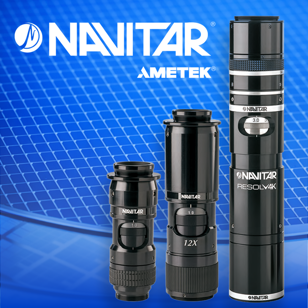
• A modular ecosystem (adapters, body tubes, illumination ports, extension options) that supports multiple recipes, like the modular Navitar Zoom 6000 Lenses
• Working distance options that maintain clearance while preserving contrast and resolution.
• Mechanical robustness and repeatability (especially if the system will be motorized).
A flexible optical platform reduces redesign risk and keeps your imaging stack relevant as processes, parts, and sensor formats evolve. For example, the Navitar Resolv4k® Lens Series provides high flexibility. The low mag end of the zoom gives wide fields of view with no sacrifice in MTF or loss of illumination, while the high mag end delivers microscope objective like resolution at extremely long working distances.
Step 3: Select the Sensor and Interface to Match Throughput and Integration Reality
After optics, camera selection becomes clearer. In semiconductor inspection, the “best” camera is the one that integrates cleanly, supports your motion model, and meets throughput targets with dependable synchronization and long-term availability.
Considerations that matter in production:
• Shutter type (global vs rolling) relative to motion and vibration.
• Interface choice (USB3, 10GigE, etc.) based on determinism, cable length, EMI environment, and synchronization.
• Mechanical footprint and thermal design, especially in space-constrained tool heads.
• Software/SDK consistency to reduce engineering overhead across variants.
The Pixelink PL-D /PL-U USB series provides a variety of sensor sizes from under 1/2" to 1.2”. When needed, the Pixelink 10 GigE Cameras provide even more through put for larger sensor formats when speed is critical.
Step 4: Make Spectral Strategy a First-Class Decision (VIS → NIR → SWIR)
Visible illumination solves many tasks, but not all. NIR and SWIR imaging can reveal subsurface structures, backside features, and material-dependent contrast differences that are difficult or impossible in the visible. If your roadmap includes silicon transmissive inspection or materials where absorption changes with wavelength, build spectral optionality into the system architecture early.
Where spectral expansion often pays off:
• Subsurface or backside inspection through silicon.
• Contrast enhancement for certain films, adhesives, or encapsulants in packaging workflows.
• Applications where visible glare dominates and longer wavelengths improve signal-to-noise.
Adding spectral capability late can force mechanical redesigns; planning for it early often means swapping components, not rebuilding the tool. The Pixelink PL-D782 Camera is a go-to camera for NIR inspection.
Step 5: Engineer for Automation and Repeatability from Day One
Automation is the economic engine of semiconductor inspection. The imaging stack must support repeatable focus and magnification changes, stable calibration, and recipe-driven operation at scale. Even if your first deployment is a lab station, decisions you make now can either enable or block future automation.
Automation-friendly design choices:
• Motorized focus/zoom readiness and repeatable positional control.
• Illumination stability and alignment-friendly mechanics.
• Calibration strategy (including detents/preset magnifications where measurement repeatability matters).
• Maintainability: access, replacement, and requalification plans for the installed base.
If you anticipate motorization later, choose platforms that already support motorized variants. Requalifying optics midstream can be more costly than selecting automation-ready options up front.
Step 6: Use Off-the-Shelf to Learn Fast, Then Customize Where Physics Demands It
Off-the-shelf components are ideal for rapid prototyping and early customer validation. They help you establish baseline performance and expose “if only” gaps, meaning “if only they had a different working distance, form factor, numerical aperture, spectral coverage, integration constraints, etc.” That is the moment to move from catalog selection to semi-custom adaptation or fully custom optical design.
Common “if only” triggers that justify customization:
• If only the working distance fit the tool envelope without sacrificing resolution.
• If only the optics maintained performance across a broader wavelength band.
• If only the mechanical package fit the OEM tool head without rework.
• If only a tube lens/attachment existed that made the whole stack click into place.
In semiconductor inspection, customization is often the shortest path to production robustness once the defect mechanism and tool constraints are fully understood.
We offer bespoke, customized solutions for everything from SWIR zoom lenses, to cameras with small form factors, to objectives, to tube lenses, to laser optics for micromachining and direct laser writing of masks. Semi-custom solutions can customize magnification, working distance, and other “if only” specifications.
A System-Level Co-Development Model
One of the fastest ways to reduce risk is to treat optics, camera, and specialized optical engineering as a coordinated design effort. When teams co-develop the stack, integration friction drops: optical performance, mechanical packaging, and software/triggering decisions are aligned from the beginning.
A practical division of responsibilities often looks like this:
•; Modular optics and zoom-based architectures to cover multiple inspection recipes and working distances.
• Industrial cameras and integration options (interfaces, footprints, SDK consistency) to match throughput and tool architecture.
• Custom and semi-custom optical engineering for objectives, tube lenses, and laser/micromachining optics when catalog solutions hit physical limits.
Semiconductor inspection requirements evolve continuously, with new materials, new packaging, and higher throughput targets. Imaging stacks that win over time are those engineered for adaptability: modular optics, automation readiness, spectral flexibility, and a clear customization path once physics sets the boundary conditions.
If you are planning an inspection upgrade or new module, consider using the six-step framework above as a checklist. It will help you move faster in the lab, integrate cleaner into production tools, and preserve optionality as your inspection roadmap matures. For guidance in selecting the best components for your system, please contact our expert application and design engineers.
Have any questions?
Speak to a member of our team today.